- 您现在的位置:买卖IC网 > Sheet目录1252 > VTERB-BLK-X2-UT4 (Lattice Semiconductor Corporation)LICENSE VITERBI DECODER XP2
�� �
�
�Lattice� Semiconductor�
�Functional� Description�
�Data� Type�
�The� Viterbi� Decoder� IP� supports� two� commonly� used� binary� representations,� namely,� sign-magnitude� and�
�unsigned� offset,� for� soft� decision� data.� In� sign-magnitude� representation,� the� most� significant� bit� is� a� sign� bit� and�
�the� rest� of� the� bits� represent� the� magnitude.� The� most� positive� number� corresponds� to� strong� logic� zero� and� other�
�positive� numbers� are� weak� logic� zeros.� The� most� negative� number� corresponds� to� strong� logic� one� and� other� neg-�
�ative� numbers� are� weak� logic� ones.� In� unsigned� offset� representation,� there� is� no� sign� bit� in� the� number� and� all�
�numbers� are� treated� positive.� The� smallest� number� (all� zeros)� corresponds� to� strong� logic� zero� and� the� biggest�
�number� (all� ones)� corresponds� to� strong� logic� one.� The� smaller� numbers� counting� up� from� zero� are� progressively�
�weaker� logic� zeros� and� bigger� numbers� counting� down� from� the� biggest� number� are� progressively� weaker� logic�
�ones.�
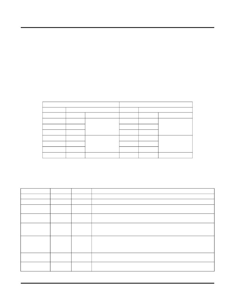
�Table� 2-2� shows� the� data� values� and� their� interpretation� in� “Signed”� and� “Unsigned”� data� type� configurations� when�
�Soft� Width� is� 3.�
�Table� 2-2.� Interpretation� of� Signed� and� Unsigned� Data�
�Signed� Binary�
�Unsigned� Offset�
�Data�
�Interpretation�
�Data�
�Interpretation�
�111�
�110�
�101�
�100�
�000�
�001�
�010�
�011�
�-3�
�-2�
�-1�
�-0�
�0�
�1�
�2�
�3�
�(strong� logic� 1)�
�(weaker� logic� 1s)�
�(weaker� logic� 0s)�
�(strong� logic� 0)�
�111�
�110�
�101�
�100�
�011�
�010�
�001�
�000�
�7�
�6�
�5�
�4�
�3�
�2�
�1�
�0�
�(strong� logic� 1)�
�(weaker� logic� 1s)�
�(weaker� logic� 0s)�
�(strong� logic� 0)�
�Signal� Descriptions�
�The� top� level� interface� diagram� of� the� Viterbi� Decoder� is� shown� in� Figure� 2-1.� The� details� of� the� I/O� ports� are� sum-�
��Table� 2-3.� Top� Level� I/O� Interface�
�Port�
�clk�
�rstn�
�pbstart�
�ibstart�
�Bits�
�1�
�1�
�1�
�1�
�I/O�
�I�
�I�
�I�
�I�
�Description�
�System� clock�
�System� wide� asynchronous� active-low� reset� signal�
�“Punctured� block� start”� signal� to� indicate� the� start� of� a� new� block� of� punctured�
�data.� This� signal� is� not� available� while� decoding� non-punctured� codes.�
�Input� block� start� signal.� This� must� be� pulled� high� when� the� first� data� of� a� block� is�
�applied� on� the� input� port.� This� port� is� available� for� block� decoding� only.�
�Input� block� end� signal.� This� signal� must� be� pulled� high� to� indicate� the� last� data�
�ibend�
�1�
�I�
�of� a� block� being� applied� on� the� input� port.� This� port� is� available� for� block� decod-�
�ing� only.�
�din0,� din1,�
�Data� input� buses� –� The� buses� become� one� bit� inputs� for� hard� decision� decoding�
�din2,� din3,�
�din4,� din5,�
�din6�
�inrate�
�outrate�
�1� or� 3�
�to� 8� (each)�
�1-4�
�2-5�
�I�
�I�
�I�
�and� equals� to� the� soft� width� for� soft� decision� decoding.� The� number� of� buses� is� 1�
�for� punctured� codes� and� n� for� non-punctured� codes,� where� n� is� the� code� rate�
�factor,� from� 2� to� 7.�
�Input� rate� of� the� convolutional� code� for� next� block.� This� port� is� available� only� in�
�dynamic� puncturing� mode.�
�Output� rate� of� the� convolutional� code� for� next� block.� This� port� is� available� only� in�
�dynamic� puncturing� mode.�
�IPUG32_02.7,� June� 2010�
�12�
�Block� Viterbi� Decoder� User’s� Guide�
�发布紧急采购,3分钟左右您将得到回复。
相关PDF资料
VTERB-DECO-XP-N1
IP CORE VITERBI DECODER XPGA
VTP110F
POLYSWITCH PTC RESET 1.1A STRAP
VTP175LF
POLYSWITCH PTC RESET 1.75A STRAP
VTP210GF
POLYSWITCH PTC RESET 2.1A STRAP
VTP210SF
POLYSWITCH PTC RESET 2.1A STRAP
W51-A121B1-10
CIRCUIT BREAKER THERM 10A ILLUM
W54-XC2A4B10-40
CIRCUIT BREAKER THERMAL 40AMP
WV-089047-10-9
LABEL ID PRODUCTS
相关代理商/技术参数
VTERB-BLK-XM-U4
功能描述:编码器、解码器、复用器和解复用器 Block Viterbi Decoder RoHS:否 制造商:Micrel 产品:Multiplexers 逻辑系列:CMOS 位数: 线路数量(输入/输出):2 / 12 传播延迟时间:350 ps, 400 ps 电源电压-最大:2.625 V, 3.6 V 电源电压-最小:2.375 V, 3 V 最大工作温度:+ 85 C 安装风格:SMD/SMT 封装 / 箱体:QFN-44 封装:Tray
VTERB-DECO-O4-N1
功能描述:编码器、解码器、复用器和解复用器 Viterbi Decoder RoHS:否 制造商:Micrel 产品:Multiplexers 逻辑系列:CMOS 位数: 线路数量(输入/输出):2 / 12 传播延迟时间:350 ps, 400 ps 电源电压-最大:2.625 V, 3.6 V 电源电压-最小:2.375 V, 3 V 最大工作温度:+ 85 C 安装风格:SMD/SMT 封装 / 箱体:QFN-44 封装:Tray
VTERB-DECO-XP-N1
功能描述:编码器、解码器、复用器和解复用器 Viterbi Decoder RoHS:否 制造商:Micrel 产品:Multiplexers 逻辑系列:CMOS 位数: 线路数量(输入/输出):2 / 12 传播延迟时间:350 ps, 400 ps 电源电压-最大:2.625 V, 3.6 V 电源电压-最小:2.375 V, 3 V 最大工作温度:+ 85 C 安装风格:SMD/SMT 封装 / 箱体:QFN-44 封装:Tray
VTESALLANF-155.520000
功能描述:155.52MHz LVPECL VCXO Oscillator Surface Mount 3.3V 100mA Enable/Disable 制造商:taitien 系列:VT 包装:剪带 零件状态:新产品 类型:VCXO 频率:155.52MHz 功能:启用/禁用 输出:LVPECL 电压 - 电源:3.3V 频率稳定度:±50ppm 工作温度:-40°C ~ 85°C 电流 - 电源(最大值):100mA 等级:- 安装类型:表面贴装 大小/尺寸:0.276" 长 x 0.197" 宽(7.00mm x 5.00mm) 高度:0.075"(1.90mm) 封装/外壳:6-SMD,无引线(DFN,LCC) 电流 - 电源(禁用)(最大值):- 标准包装:200
VTESFP4G
制造商:Promise Technologies 功能描述:SP.VTRAK.4GB SFP OPTICAL TRANSCEIVER.BOX - Bulk
VTEUALJANF-122.880000
功能描述:122.88MHz CMOS VCXO Oscillator Surface Mount 3.3V 40mA Enable/Disable 制造商:taitien 系列:VT 包装:剪带 零件状态:新产品 类型:VCXO 频率:122.88MHz 功能:启用/禁用 输出:CMOS 电压 - 电源:3.3V 频率稳定度:±50ppm 工作温度:-40°C ~ 85°C 电流 - 电源(最大值):40mA 等级:- 安装类型:表面贴装 大小/尺寸:0.276" 长 x 0.197" 宽(7.00mm x 5.00mm) 高度:0.075"(1.90mm) 封装/外壳:6-SMD,无引线(DFN,LCC) 电流 - 电源(禁用)(最大值):- 标准包装:200
VTEUALJANF-153.600000
功能描述:153.6MHz CMOS VCXO Oscillator Surface Mount 3.3V 40mA Enable/Disable 制造商:taitien 系列:VT 包装:剪带 零件状态:新产品 类型:VCXO 频率:153.6MHz 功能:启用/禁用 输出:CMOS 电压 - 电源:3.3V 频率稳定度:±50ppm 工作温度:-40°C ~ 85°C 电流 - 电源(最大值):40mA 等级:- 安装类型:表面贴装 大小/尺寸:0.276" 长 x 0.197" 宽(7.00mm x 5.00mm) 高度:0.075"(1.90mm) 封装/外壳:6-SMD,无引线(DFN,LCC) 电流 - 电源(禁用)(最大值):- 标准包装:200
VTEUALJANF-30.720000
功能描述:30.72MHz CMOS VCXO Oscillator Surface Mount 3.3V 20mA Enable/Disable 制造商:taitien 系列:VT 包装:剪切带(CT) 零件状态:新产品 类型:VCXO 频率:30.72MHz 功能:启用/禁用 输出:CMOS 电压 - 电源:3.3V 频率稳定度:±50ppm 工作温度:-40°C ~ 85°C 电流 - 电源(最大值):20mA 等级:- 安装类型:表面贴装 大小/尺寸:0.276" 长 x 0.197" 宽(7.00mm x 5.00mm) 高度:0.075"(1.90mm) 封装/外壳:6-SMD,无引线(DFN,LCC) 电流 - 电源(禁用)(最大值):- 标准包装:1